

The Keolabs EMVCo L1 test solution supports RF and protocol layer testing for EMVCo L1 contactless cards and terminals, meets the new EMVCo specification requirements, and has been authorized by the EMVCo organization. It is the preferred EMVCo testing equipment in the industry.
EMVCo Level 1 PICC Analog test suite
EMVCo Level 1 PICC Digital test suite
EMVCo Level 1 Mobile Analog test suite
EMVCo Level 1 PCD Analog test suite
EMVCo Level 1 PCD Digital test suite
EMVCo Level 1 Reduced Range Terminal Analog test suite
At KEOLABS, all our platforms and solutions are EMVCo qualified.
EMV™ is the global standard for payment cards and readers based on contact and contactless smart card technologies. The EMV specifications encompass test procedures and compliance processes managed by EMVCo, an organisation jointly owned and operated by American Express, Discover, JCB, MasterCard, UnionPay and Visa.
KEOLABS provides complete testing solutions developed and qualified in accordance with EMVCo requirements.

EMVCo Test suite for PICC Analog
• EMV Contactless Card Level 1 Type Approval – PICC Analogue Test Bench and Test Case Requirements, Version 3.2b, January 2025
EMVCo Test suite for PICC Digital
• EMV® Level 1 Specifications for Payment Systems - EMV® Contactless Interface Specification", Version 3.2 - July 2022
• EMV® Contactless Card Level 1 Type Approval - PICC Digital Test Cases", Version 3.2b - January 2025
• EMV® Mobile Product Level 1 Type Approval - Mobile L1 Test Guidelines", Version 3.2b - January 2025
EMVCo Test suite for Mobile Analog
• EMV Contactless Card Level 1 Type Approval – PICC Analogue Test Bench and Test Case Requirements, Version 3.2b, January 2025
• Mobile L1 Test Guidelines, Version 3.2b, January 2025
EMVCo Test suite for PCD Analog
• EMV® Level 1 Specifications for Payment Systems - EMV® Contactless Interface Specification, Version 3.2 - July 2022
• EMV® Contactless Terminal Level 1 Type Approval - PCD Analogue Test Bench and Test Case Requirements, Version 3.2a - January 2025
EMVCo Test suite for PCD Digital
• EMV® Level 1 Specifications for Payment Systems - EMV® Contactless Interface Specification" - Version 3.2 - July 2022
• EMV® Contactless Terminal Level 1 Type Approval – PCD Digital Test Cases", Version 3.2a - January 2025
EMVCo Test suite for Reduced Range Terminal Analog
• EMVCo Contactless Terminal Level 1 Type Approval PCD Analogue Test Bench and Test Case Requirements, Version 3.1a, September 2021
• EMV RR L1 Test Guidelines, version 3.1a, September 2023
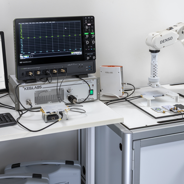
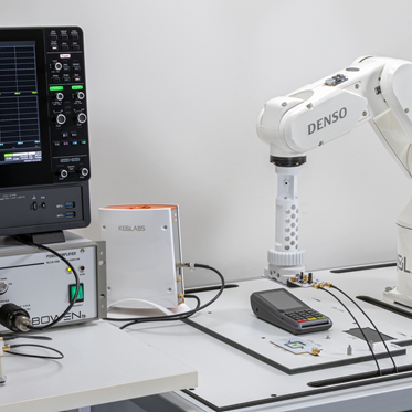
1 SCRIPTIS™ Test Environment
1 EMVCo L1 PCD Analog Test suite
1 EMVCo L1 PCD Digital Test suite
1 EMVCo L1 Reduced Range Analog Test suite

1 ProxiLAB QUEST tester with PICC Analog and Digital options

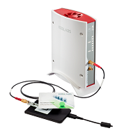
1 EMVCo Accessory set:
• SC-EMVCo Test PICC V3.0:Kit of 3 EMVCo PICC tuned at 3 frequencies (2 antennas class 1 tuned at 13.56 & 16.1MHz and 1 class 3 tuned at 13.56MHz.
• SC-EMVCo Test PCD V3.0:one EMVCo PCD antenna.

• SC-EMVCo KIT:In addition of the 3 EMVCo PICC references and the PCD antenna, 1 stand to mount the Test PCD with stackers and 1 CMR to condition the signals and switching them between its inputs and outputs for test bench set-ups are added.

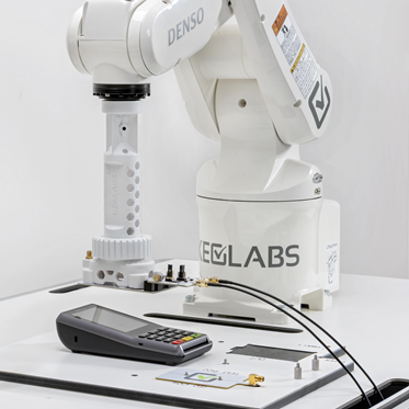
1 Robot 6 axis with dedicated accessories (optional)

1 Robot 5 axis with dedicated accessories (optional)

1 Lecroy HDO 6034-B Oscilloscope with Xdev option

1 Amplifier 50W, 10-250 MHz

This EMVCo PCD Analog test suite is compatible with the following standard:
EMV® Level 1 Specifications for Payment Systems - EMV® Contactless Interface Specification, Version 3.2 - July 2022
EMV® Contactless Terminal Level 1 Type Approval - PCD Analogue Test Bench and Test Case Requirements, Version 3.2a - January 2025
Our coverage of this test specification includes the following test cases (numbering according to the EMVCo version 3.2a):
Radio Frequency Power
• §8.8.1.1. TAB111.zrf - Verifying the PCD to PICC Power Transfer
• §8.8.1.2. TAB112.200 - Verifying the PCD Carrier Frequency
• §8.8.1.3. TAB113.200 - Verifying the PCD Operating Field Resetting
• §8.8.1.4. TAB114.200 - Verifying the PCD Power-Off of the Operating Field
• §8.8.1.5. TAB115.200 - Verifying the Polling sequence when supporting other technologies
• §8.8.1.6. TAB116.200 - Verifying the Suspend of PCD Operating Field
PCD to PICC Signal Interface for Type A Communications
• §8.8.2.x. TA12x.z00 - Verifying the PCD Timing
PICC to PCD Signal Interface for Type A Communications
• §8.8.3.1. TA131.zrf - Verifying the Load Modulation VS1,pp at Minimum Positive Modulation
• §8.8.3.2. TA132.zrf - Verifying the Load Modulation VS2,pp at Minimum Positive Modulation
• §8.8.3.3. TA133.zrf - Verifying the Load Modulation VS1,pp at Maximum Positive Modulation
• §8.8.3.4. TA134.zrf - Verifying the Load Modulation VS2,pp at Maximum Positive Modulation
• §8.8.3.5. TA135.zrf - Verifying the Load Modulation VS1,pp at Minimum Negative Modulation
• §8.8.3.6. TA136.zrf - Verifying the Load Modulation VS2,pp at Minimum Negative Modulation
• §8.8.3.7. TA137.zrf - Verifying the Load Modulation VS1,pp at Maximum Negative Modulation
• §8.8.3.8. TA138.zrf - Verifying the Load Modulation VS2,pp at Maximum Negative Modulation
• §8.8.3.9. TA139.000 - Verifying the FDTA,PICC tolerance
Bit Level Coding Signal Interface for Type A Communications
• §8.8.4.1. TA141.1.3.200 - Verifying the PCD Transmitted Bit Rate
• §8.8.4.2. TA142.1.3.200 - Verifying the Bit Coding and De-synchronization PCD to PICC
• §8.8.4.3. TA143.1.3.200 - Verifying the Bit Coding and De-synchronization PICC to PCD
PCD IQ Demodulation for Type A communications
• §8.8.8.1. TA151.200 Verifying the PCD IQ Demodulation
PCD to PICC Signal Interface for Type B Communications
• §8.8.5.x. TB12x.z00 - Verifying the PCD Timing
PICC to PCD Signal Interface for Type B Communications
• §8.8.6.1. TB131.zrf - Verifying the Load Modulation VS1,pp at Minimum Positive Modulation
• §8.8.6.2. TB132.zrf - Verifying the Load Modulation VS2,pp at Minimum Positive Modulation
• §8.8.6.3. TB133.zrf - Verifying the Load Modulation VS1,pp at Maximum Positive Modulation
• §8.8.6.4. TB134.zrf - Verifying the Load Modulation VS2,pp at Maximum Positive Modulation
• §8.8.6.5. TB135.zrf - Verifying the Load Modulation VS1,pp at Minimum Negative Modulation
• §8.8.6.6. TB136.zrf - Verifying the Load Modulation VS2,pp at Minimum Negative Modulation
• §8.8.6.7. TB137.zrf - Verifying the Load Modulation VS1,pp at Maximum Negative Modulation
• §8.8.6.8. TB138.zrf - Verifying the Load Modulation VS2,pp at Maximum Negative Modulation
Bit Level Coding Signal Interface for Type B Communications
• §8.8.7.1. TB141.200 - Verifying the PCD Transmitted Bit Rate
• §8.8.7.2. TB142.200 - Verifying the Synchronization, Bit Coding and Desynchronization of PCD to PICC
• §8.8.7.3. TB145.200 - Verifying the Maximum Limit De-synchronization PICC to PCD (tFSOFF,MAX)
• §8.8.7.4. TB147.200 - Verifying the Bit Boundaries with Type B Communications
• §8.8.7.5. TB148.200 - Verifying the Minimum Limit De-synchronization PICC to PCD (tFSOFF,MIN)
PCD IQ Demodulation for Type B communications
• §8.8.8.1. TB151.200 Verifying the PCD IQ Demodulation
This EMVCo PCD Digital test suite is compatible with the following standard:
EMV® Level 1 Specifications for Payment Systems - EMV® Contactless Interface Specification" - Version 3.2 - July 2022
EMV® Contactless Terminal Level 1 Type Approval – PCD Digital Test Cases", Version 3.2a - January 2025
Our coverage of this test specification includes the following test cases (numbering according to the EMVCo version 3.2a):
Type A Tests:
• §4.1. TA001 - Basic Type A Exchange (single size UID) and timings measurement
• §4.2. TA002 - Type A Correct Removal
• §4.3. TA003.x - Basic Type A Exchange with the minimum and the default maximum Frame Delay Time PCD to PICC
• §4.4. TA004.x - Type A Correct Presence Check
• §4.5. TA101.x - Type A Installation with double and triple UID size
• §4.6. TA102.x - Type A Installation with supported values of ATQA
• §4.7. TA103.x - Type A Installation with supported values of SAK and of the TA(1) byte of the ATS
• §4.8. TA104.xy - Type A Installation with supported values of the TL byte (and historical bytes) of the ATS
• §4.9. TA105.xy - Type A Installation with supported values of SFGI in the TB(1) byte of the ATS
• §4.10. TA106.x - Type A Installation with supported values of the TC(1) byte of the ATS
• §4.11. TA108 - Type A Installation with Type A frame answered to HLTA command
• §4.12. TA110.x - Type A Installation with different values of ATQA
• §4.13 TA112.x - Type A Installation with ‘noise’ after each PICC response
• §4.14. TA201.xy - Type A Error free non-chained I-Blocks exchanges for all possible values of FWT
• §4.15. TA202.xy - Type A Error free chained I-Blocks in both directions for different values of FSC
• §4.16. TA203.xy - Type A Error free chained I-Blocks transmission for FSC = 16 to 256 bytes
• §4.17. TA204.x - Type A Error free request for Frame Waiting Time Extension on nonchained I-Blocks
• §4.18. TA205.x - Type A Error free request for Frame Waiting Time Extension during chaining in both directions
• §4.19. TA206 - Type A Error free chained I-Blocks in both directions with different values of FSD
• §4.20. TA210 - Type A Error free chained I-Blocks reception with rare frame sizes
• §4.21. TA215.x - Type A Error free exchange with the minimum Frame Delay Time PCD to PICC for different values of the Frame Waiting Time
• §4.22. TA216.x Type A I-Blocks exchange and request for Frame Waiting Time Extension with ‘noise’ after each PICC response
• §4.23. TA301.xy - Type A Polling with an error after WUPA
• §4.24. TA302.xy - Type A Collision detection with an error after ANTICOLLISION CL1
• §4.25. TA303 - Type A Polling with detection of a Type A then a Type B PICC
• §4.26. TA304.xy - Type A Collision detection with an error after WUPA
• §4.27. TA305.xy - Type A Collision detection with an error after SELECT CL1
• §4.28. TA306.xy - Type A Activation with an error after RATS
• §4.29. TA307.x - Type A Activation with ‘noise’ after RATS
• §4.30. TA310 - Type A Collision detection with a time-out after ANTICOLLISION CL1
• §4.31. TA311.x - Type A Collision detection with a time-out after WUPA
• §4.32. TA312 - Type A Collision detection with a time-out after SELECT CL1
• §4.33. TA313 - Type A Activation with a time-out after RATS
• §4.34. TA335.xy - Type A Activation with respect of the EMD Suppression behavior after RATS
• §4.35. TA340.x - Type A Activation with respect of the ‘deaf time’ after RATS
• §4.36. TA401.xy - Type A Error notification on an I-Block not indicating chaining
• §4.37. TA402 - Type A Time-out after an I-Block not indicating chaining
• §4.38. TA403.x - Type A Transmission error in response to an I-Block not indicating chaining
• §4.39. TA404.xy - Type A Protocol error in response to an I-Block not indicating chaining
• §4.40. TA405.xy - Type A Error notification on an I-Block indicating chaining
• §4.41. TA406 - Type A Time-out after an I-Block indicating chaining
• §4.42. TA407.x - Type A Transmission error in response to an I-Block indicating chaining
• §4.43. TA408.xy - Type A Protocol error in response to an I-Block indicating chaining
• §4.44. TA409.xy - Type A Time-out after an R(ACK) Block (i.e. error notification)
• §4.45. TA410.x - Type A Transmission error in response to an R(ACK) Block
• §4.46. TA411.xy - Type A Protocol error in response to an R(ACK) Block
• §4.47. TA412.xy - Type A Single time-out after an S(WTX) Response Block (several values of WTXM)
• §4.48. TA413 - Type A Repeated use of a FWT Extension after a single S(WTX) Request
• §4.49. TA414.x - Type A ‘Noise’ in response to an I-Block not indicating chaining
• §4.50. TA415.x - Type A ‘Noise’ in response to an I-Block indicating chaining
• §4.51. TA416.x - Type A ‘Noise’ in response to an R(ACK) Block
• §4.52. TA417.xy - Type A Protocol error in response to an R(NAK)-Block sent to notify a transmission error
• §4.53. TA419.x - Type A Presence Check with an error after R(NAK)
• §4.54. TA420 - Type A Removal with an error after WUPA
• §4.55. TA421 - Type A Consecutive time-outs after S(WTX) Response Blocks
• §4.56. TA430.xy - Type A Block protocol with respect of the EMD suppression behavior
• §4.57. TA435.x - Type A Block Protocol with respect of the ‘deaf time’
• §4.58. TA440 - Type A Parity error in the first 4 bytes of a sequence in response to an I-Block not indicating chaining
• §4.59. TA441 - Type A Parity error in the first 4 bytes of a sequence in response to an I-Block indicating chaining
• §4.60. TA442 - Type A Parity error in the first 4 bytes of a sequence in response to an R(ACK) Block
• §4.61. TA443 - Type A Parity error in the first 4 bytes of a sequence in response to an S(WTX) Response Block
Type B Tests:
• §5.1. TB000 - Type B Pre-test to determine TR1PUTMIN
• §5.2. TB001 - Basic Type B Exchange and timings measurement
• §5.3. TB002.x - Basic Type B Exchange with supported SoS and EoS
• §5.4. TB003 - Type B Correct Removal
• §5.5. TB004.x - Basic Type B Exchange with the minimum and the default maximum Frame Delay Time PCD to PICC
• §5.6. TB006.x - Basic Type B Exchange with the minimum and the maximum characterto-character delay
• §5.7. TB007.x - To ensure that the PCD respects the timings and the series of commands during the presence check procedure of a Type B PICC.
• §5.8. TB101.x - Type B Installation with supported values of ADC
• §5.9. TB102.x - Type B Installation with supported values of FO
• §5.10. TB104.x - Type B Installation with supported values of Bit_Rate_Capability
• §5.11. TB106.x - Type B Installation with supported values of ADF
• §5.12. TB107.x - Type B Installation with supported values of b4-b2 of Protocol_Type
• §5.13. TB108.x - Type B Installation with supported values of MBLI
• §5.14. TB110.x - Type B Installation with different values of ATQB
• §5.15. TB201.xy - Type B Error free non-chained I-Blocks exchanges for all possible values of FWT
• §5.16. TB202.xy - Type B Error free chained I-Blocks in both directions for different values of FSC
• §5.17. TB203.xy - Type B Error free chained I-Blocks transmission for FSC = 16 to 256 bytes
• §5.18. TB204.x - Type B Error free request for Frame Waiting Time Extension on nonchained I-Blocks
• §5.19. TB205.x - Type B Error free request for Frame Waiting Time Extension during chaining in both directions
• §5.20. TB206 - Type B Error free chained I-Blocks in both directions with different values of FSD
• §5.21. TB210 - Type B Error free chained I-Blocks reception with rare frame sizes
• §5.22. TB215.x - Type B Error free exchange with the minimum Frame Delay Time PCD to PICC for different values of the Frame Waiting Time
• §5.23. TB301.xy - Type B Polling with an error after WUPB
• §5.24. TB303 - Type B Polling with detection of a Type B then a Type A PICC
• §5.25. TB304.xy - Type B Collision detection with an error after WUPB
• §5.26. TB305.x - Type B Activation with ‘noise’ after ATTRIB
• §5.27. TB306.xy - Type B Activation with an error after ATTRIB
• §5.28. TB311.x - Type B Collision detection with a time-out after WUPB
• §5.29. TB312.x - Type B Activation with a time-out after ATTRIB
• §5.30 TB335.xy - Type B Activation with respect of the EMD Suppression behavior after ATTRIB
• §5.31. TB340.x - Type B Activation with respect of the ‘deaf time’ after ATTRIB
• §5.32. TB401.xy - Type B Error notification on an I-Block not indicating chaining
• §5.33. TB402 - Type B Time-out after an I-Block not indicating chaining
• §5.34. TB403.x - Type B Transmission error in response to an I-Block not indicating chaining
• §5.35. TB404.xy - Type B Protocol error in response to an I-Block not indicating chaining
• §5.36. TB405.xy - Type B Error notification on an I-Block indicating chaining
• §5.37. TB406 - Type B Time-out after an I-Block indicating chaining
• §5.38. TB407 - Type B Transmission error in response to an I-Block indicating chaining
• §5.39. TB408.xy - Type B Protocol error in response to an I-Block indicating chaining
• §5.40. TB409.xy - Type B Time-out after an R(ACK) Block (i.e. error notification)
• §5.41. TB410.x - Type B Transmission error in response to an R(ACK) Block
• §5.42. TB411.xy - Type B Protocol error in response to an R(ACK) Block
• §5.43. TB412.xy - Type B Single time-out after an S(WTX) Response Block (several values of WTXM)
• §5.44. TB413 - Type B Repeated use of a FWT extension after a single S(WTX) Request
• §5.45. TB414.x - Type B ‘Noise’ in response to an I-Block not indicating chaining
• §5.46. TB415.x - Type B ‘Noise’ in response to an I-Block indicating chaining
• §5.47. TB415.x - Type B ‘Noise’ in response to an R(ACK) Block
• §5.48. TB417.xy - Type B Protocol error in response to an R(NAK)-Block sent to notify a transmission error
• §5.49. TB419.x - Type B Presence Check with an error after R(NAK)
• §5.50. TB420 - Type B Removal with an error after WUPB
• §5.51. TB421 - Type B Consecutive time-outs after S(WTX) Response Blocks
• §5.52. TB430.xy - Type B Block protocol with respect of the EMD suppression behavior
• §5.53. TB435.x - Type B Block Protocol with respect of the ‘deaf time’
This EMVCo PCD Analogue test suite is compatible with the following standard:
EMVCo Contactless Terminal Level 1 Type Approval PCD Analogue Test Bench and Test Case Requirements, Version 3.1a, September 2021
EMV RR L1 Test Guidelines, version 3.1a, September 2023
This test suite also includes the EMVCo certified Scoring tool based on the “EMV Terminal Type Approval Bulletin No. 276, First Edition April 2024 – Reduced Range Devices Acceptance Criteria“.
Radio Frequency Power
• §8.8.1.1. TAB111.zrf - Verifying the PCD to PICC Power Transfer
• §8.8.1.2. TAB112.200 - Verifying the PCD Carrier Frequency
• §8.8.1.3. TAB113.200 - Verifying the PCD Operating Field Resetting
• §8.8.1.4. TAB114.200 - Verifying the PCD Power-Off of the Operating Field
• §8.8.1.5. TAB115.200 - Verifying the Polling sequence when supporting other technologies
PCD to PICC Signal Interface for Type A Communications
• §8.8.2.x. TA12x.z00 - Verifying the PCD Timing
PICC to PCD Signal Interface for Type A Communications
• §8.8.3.1. TA131.zrf - Verifying the Load Modulation VS1,pp at Minimum Positive Modulation
• §8.8.3.2. TA132.zrf - Verifying the Load Modulation VS2,pp at Minimum Positive Modulation
• §8.8.3.3. TA133.zrf - Verifying the Load Modulation VS1,pp at Maximum Positive Modulation
• §8.8.3.4. TA134.zrf - Verifying the Load Modulation VS2,pp at Maximum Positive Modulation
• §8.8.3.5. TA135.zrf - Verifying the Load Modulation VS1,pp at Minimum Negative Modulation
• §8.8.3.6. TA136.zrf - Verifying the Load Modulation VS2,pp at Minimum Negative Modulation
• §8.8.3.7. TA137.zrf - Verifying the Load Modulation VS1,pp at Maximum Negative Modulation
• §8.8.3.8. TA138.zrf - Verifying the Load Modulation VS2,pp at Maximum Negative Modulation
• §8.8.3.9. TA139.000 - Verifying the FDTA,PICC tolerance
Bit Level Coding Signal Interface for Type A Communications
• §8.8.4.1. TA141.1.3.200 - Verifying the PCD Transmitted Bit Rate
• §8.8.4.2. TA142.1.3.200 - Verifying the Bit Coding and De-synchronization PCD to PICC
• §8.8.4.3. TA143.1.3.200 - Verifying the Bit Coding and De-synchronization PICC to PCD
PCD IQ Demodulation for Type A communications
• §8.8.8.1. TA151.200 Verifying the PCD IQ Demodulation
PCD to PICC Signal Interface for Type B Communications
• §8.8.5.x. TB12x.z00 - Verifying the PCD Timing
PICC to PCD Signal Interface for Type B Communications
• §8.8.6.1. TB131.zrf - Verifying the Load Modulation VS1,pp at Minimum Positive Modulation
• §8.8.6.2. TB132.zrf - Verifying the Load Modulation VS2,pp at Minimum Positive Modulation
• §8.8.6.3. TB133.zrf - Verifying the Load Modulation VS1,pp at Maximum Positive Modulation
• §8.8.6.4. TB134.zrf - Verifying the Load Modulation VS2,pp at Maximum Positive Modulation
• §8.8.6.5. TB135.zrf - Verifying the Load Modulation VS1,pp at Minimum Negative Modulation
• §8.8.6.6. TB136.zrf - Verifying the Load Modulation VS2,pp at Minimum Negative Modulation
• §8.8.6.7. TB137.zrf - Verifying the Load Modulation VS1,pp at Maximum Negative Modulation
• §8.8.6.8. TB138.zrf - Verifying the Load Modulation VS2,pp at Maximum Negative Modulation
Bit Level Coding Signal Interface for Type B Communications
• §8.8.7.1. TB141.200 - Verifying the PCD Transmitted Bit Rate
• §8.8.7.2. TB142.200 - Verifying the Synchronization, Bit Coding and Desynchronization of PCD to PICC
• §8.8.7.3. TB145.200 - Verifying the Maximum Limit De-synchronization PICC to PCD (tFSOFF,MAX)
• §8.8.7.4. TB147.200 - Verifying the Bit Boundaries with Type B Communications
• §8.8.7.5. TB148.200 - Verifying the Minimum Limit De-synchronization PICC to PCD (tFSOFF,MIN)
PCD IQ Demodulation for Type B communications
• §8.8.8.1. TB151.200 Verifying the PCD IQ Demodulation
Scriptis supports Python editing and modifying scripts:

Scriptis saves test logs in TXT format:

Scriptis saves test logs in xgpa format:

Scriptis saves test logs in xdata format:

Scriptis supports exporting reports in html format:

The Keolabs Solution by ABE supports verifying the following standards:
• EMV® Type Approval - Contactless Terminal Level 1
• EMV® Type Approval - Contactless Card Level 1
• NFC Forum Test Cases for Analog and Digital Protocol
• ISO/IEC 10373-6 Test Methods
• ISO/IEC 18745-2 Test Methods for the contactless interface
• CEN/TS 16794-2:2017 Public transport - Communication between contactless readers and fare media - Part 2: Test plan for ISO/IEC 14443
KEOLABS provides a complete testing solution that supports internal validation of smart cards and card readers based on industry standards for specific application types, including:
• Payment: Qualified solution to verify you payment applications - Used by EMVCo Laboratories
EMVCo Level 1 PCD Analog Test Suite
EMVCo Level 1 PCD Digital Test Suite
EMVCo Level 1 Reduced Range Terminal Analog Test Suite
EMVCo Level 1 PICC Analog Test Suite
EMVCo Level 1 PICC Digital Test Suite
EMVCo Level 1 Mobile Analog Test Suite
• ePassport & eID Products: Solution to verify your Identity Applications - Used by National Printing Companies
ISO 10373-6/ISO 18745-2 PICC Analog Test Suite
ISO 10373-6/ISO 18745-2 PICC Digital Test Suite
ePassport-eMRTD Application Test Suite
eID - Application EAC V2 & IAS ECC Test suites
eDL - Application ISO 18013-4 Test suite
• Access Control, Transport & Smart Objects: Solution to verify your Transport or Access Control Applications - Used by transport operators
ISO 10373-6 PICC Analog Test Suite
ISO 10373-6 PICC Digital Test Suite
ISO 10373-6 PCD Analog Test Suite
ISO 10373-6 PCD Digital Test Suite
• Mobile, Automotive Makers: Qualified solution to Verify your NFC Applications - Used by Mobile or automotive Makers
NFC Forum Poller&Listener Analog Test Suite
NFC Forum Poller&Listener Digital Test Suite
NFC Forum LLCP/SNEP test suite(Initiator/Target)

Current Products:EMV L1 PCD Test Solutions


 Back
Back